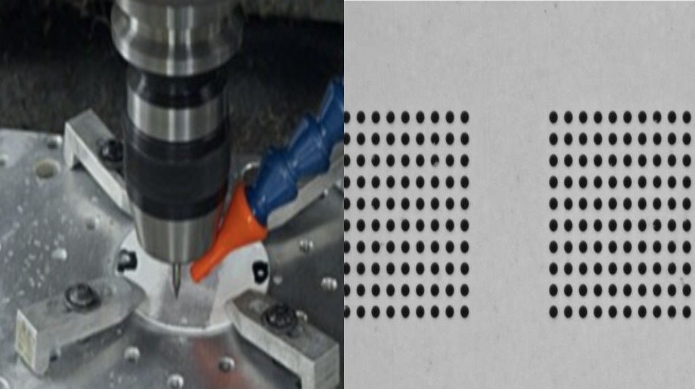
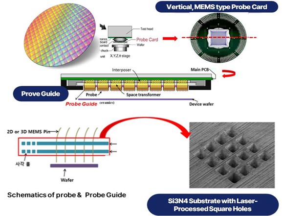
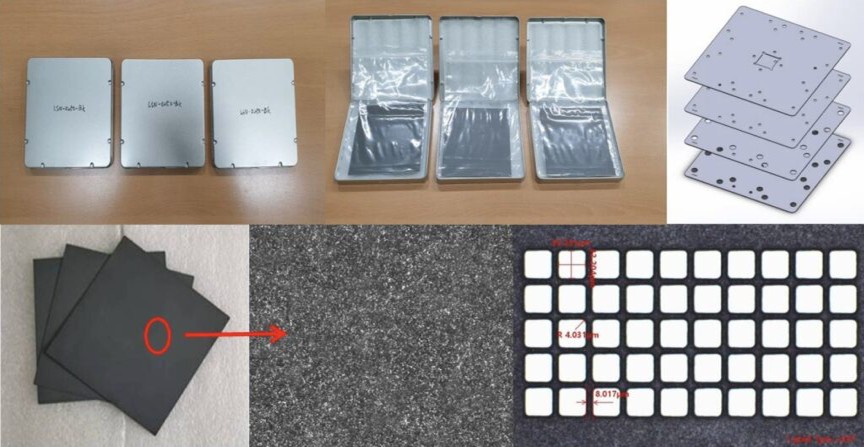
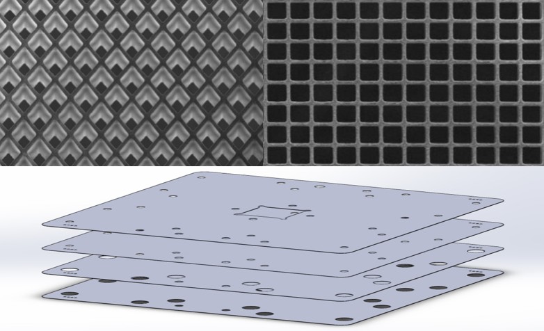
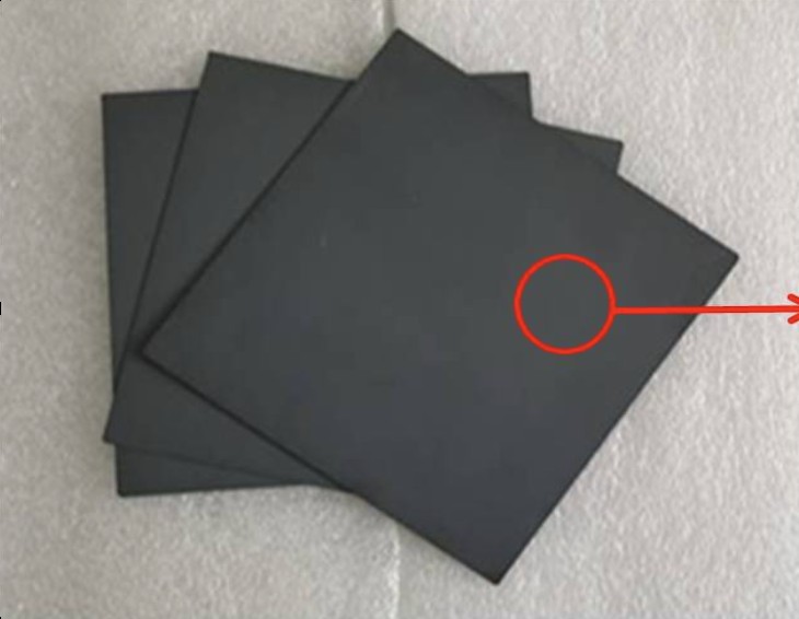
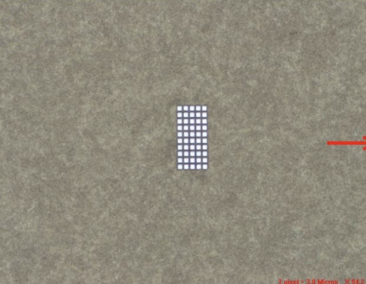
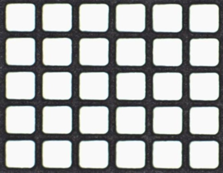
Advanced inspection equipment requires precision probe guides with ultra-fine laser-processed square holes on silicon nitride substrates. This component is essential for guiding probes with high durability and heat resistance, making it a critical and increasingly in-demand solution
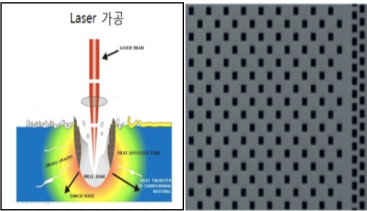
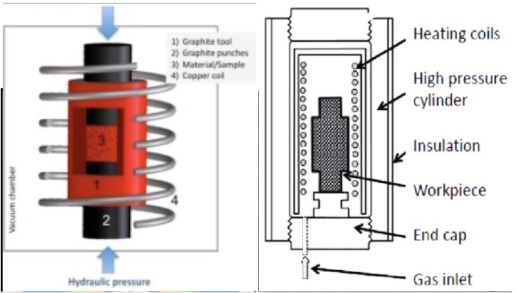
The stringent specifications and complex manufacturing process of silicon nitride substrates for semiconductor inspection equipment are currently dominated by a few foreign competitors. Their methods involve high-cost, high-temperature, and high-pressure techniques, leading to expensive products and limited supply
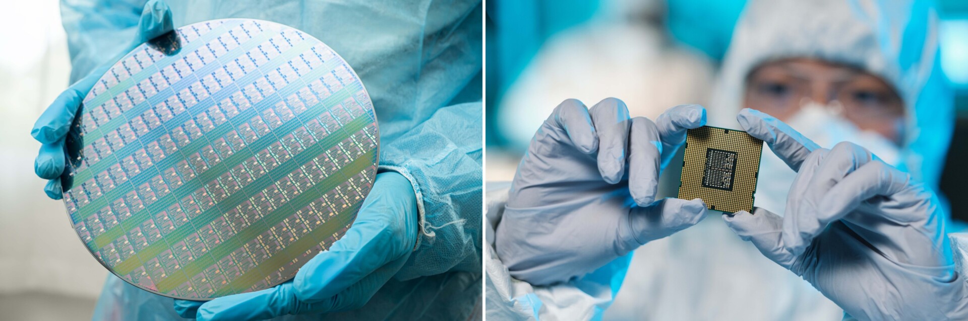
5G/AI Semiconductor Demand
Rising Demand for High-Spec 5G/AI Semiconductors
Circular Probe Equipment
Ceramic Probe Guides for Standard Semiconductor Inspection Equipment with Circular Probes
Square-Hole Probe Demand
Increasing Demand for Square-Hole Probe Guides for High-Spec Semiconductors
Production Costs
High-Cost, High-Temperature Silicon Nitride Production Methods by Overseas Competitors
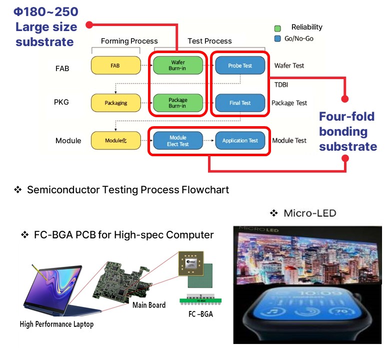
Plans for Entry into New Markets and Applications for Silicon Nitride Materials : FC-BGA BBT, Burn-in test, Probe Cleaner
: Expansion in advanced semiconductor and hydrogen fuel cell applications, including high-spec ceramic heaters
R&D and Next-Generation Product Line
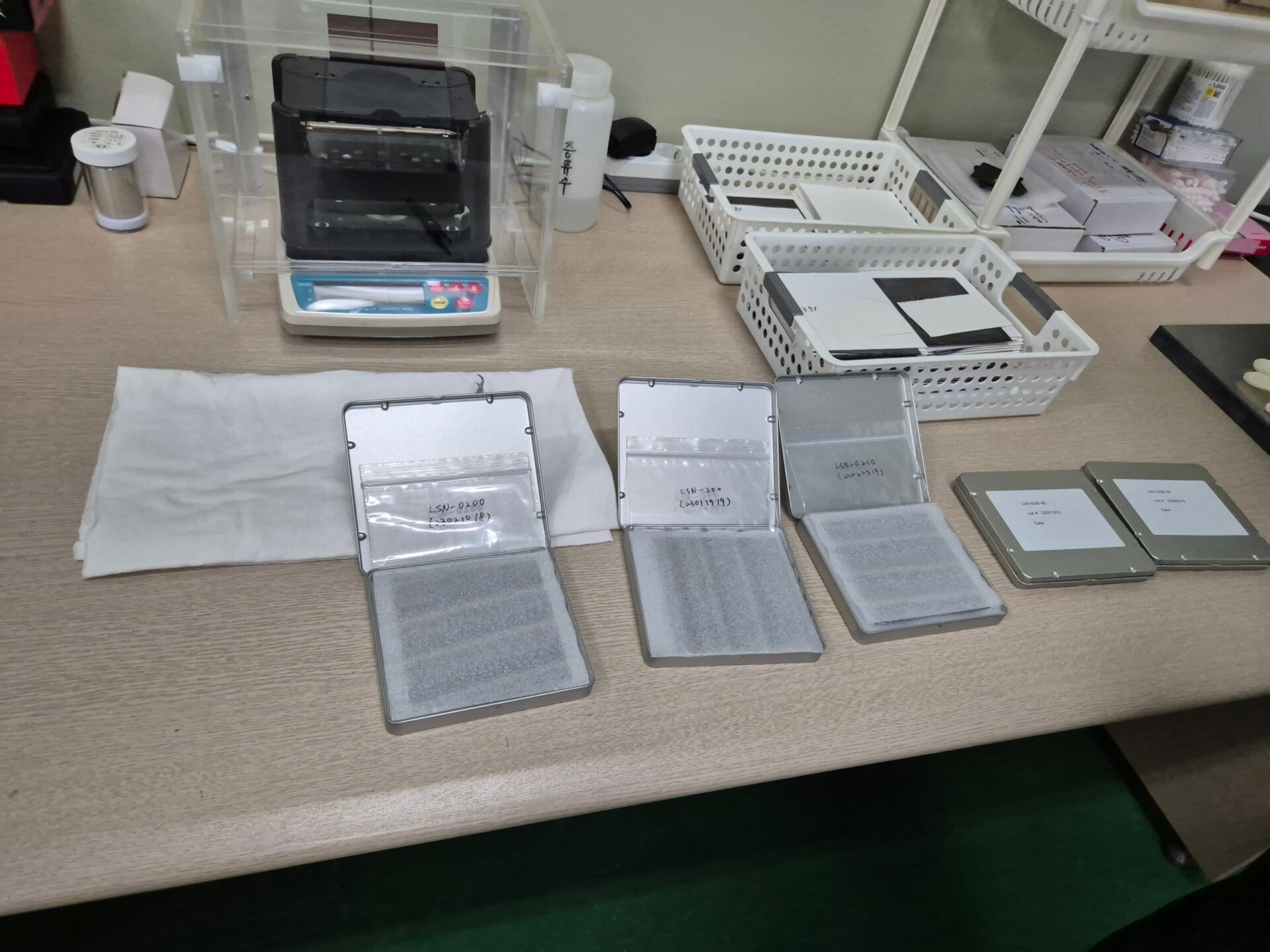
Burn in test, FC-BGA, Micro-LED inspection Probe Guide Plate
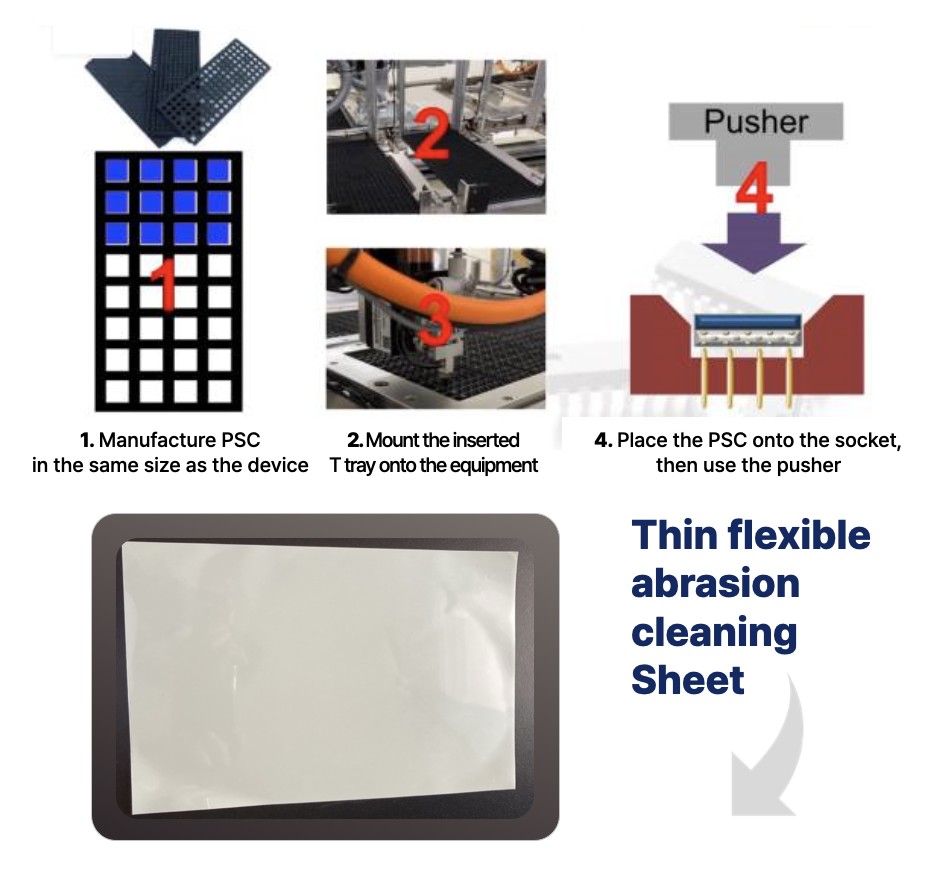
Probe Cleaning Sheet
OUR PROCESS
About LSSM
LSSM Co., Ltd. is a specialized manufacturing venture focused on producing probe guides for semiconductor inspection equipment. These guides are made using silicon nitride substrates, featuring ultra-fine laser-processed square holes for high precision.
Our company leverages proprietary material composition and low-cost differentiated manufacturing facilities and processes to deliver high-quality products that meet or exceed those of advanced foreign competitors. By reducing equipment investment costs and enhancing raw material and price competitiveness, we have developed a robust foundation for competing in the global market.
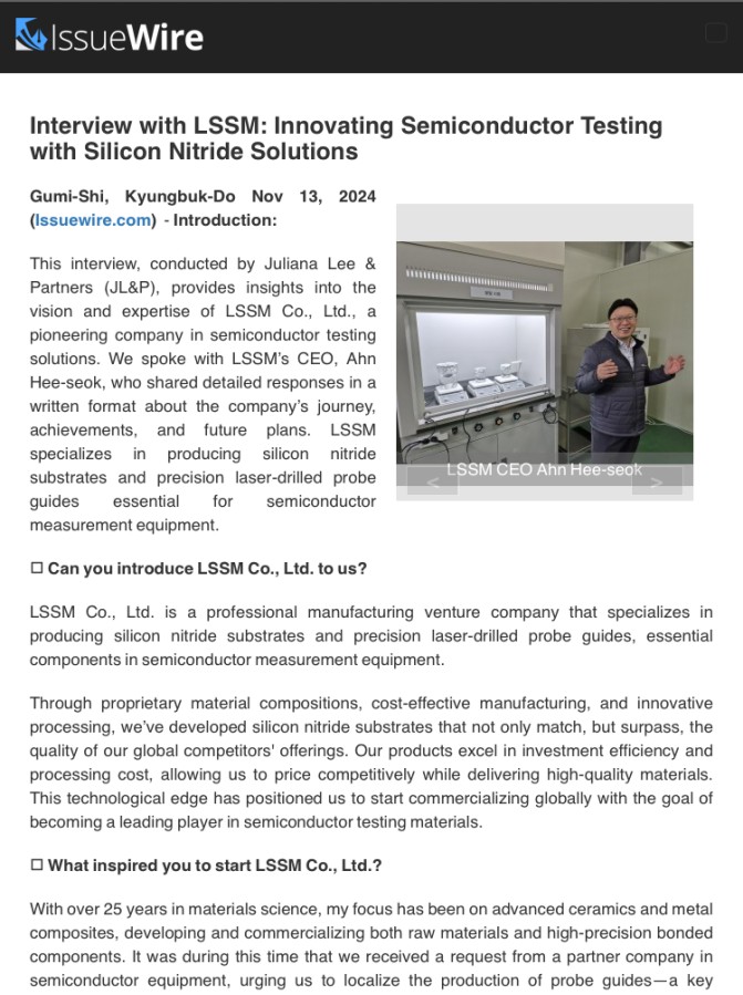
Ahn Hee-seok
CEO Head of Research
Key Personnel
Ahn Hee-seok
CEO
Head of Research
Master’s in New Materials from Hanyang University
25 years of experience in materials field
Formerly with KIST, specializing in thin film processing
Jeon Myung-pyo
Technical Expert
Ph.D. in Ceramics from KAIST
Former researcher at the Korea Institute of Ceramic Engineering and Technology
Marketing & Sales
Marketing Specialist
Master’s in Business Administration (Marketing)
26 years of experience in semiconductor-related marketing
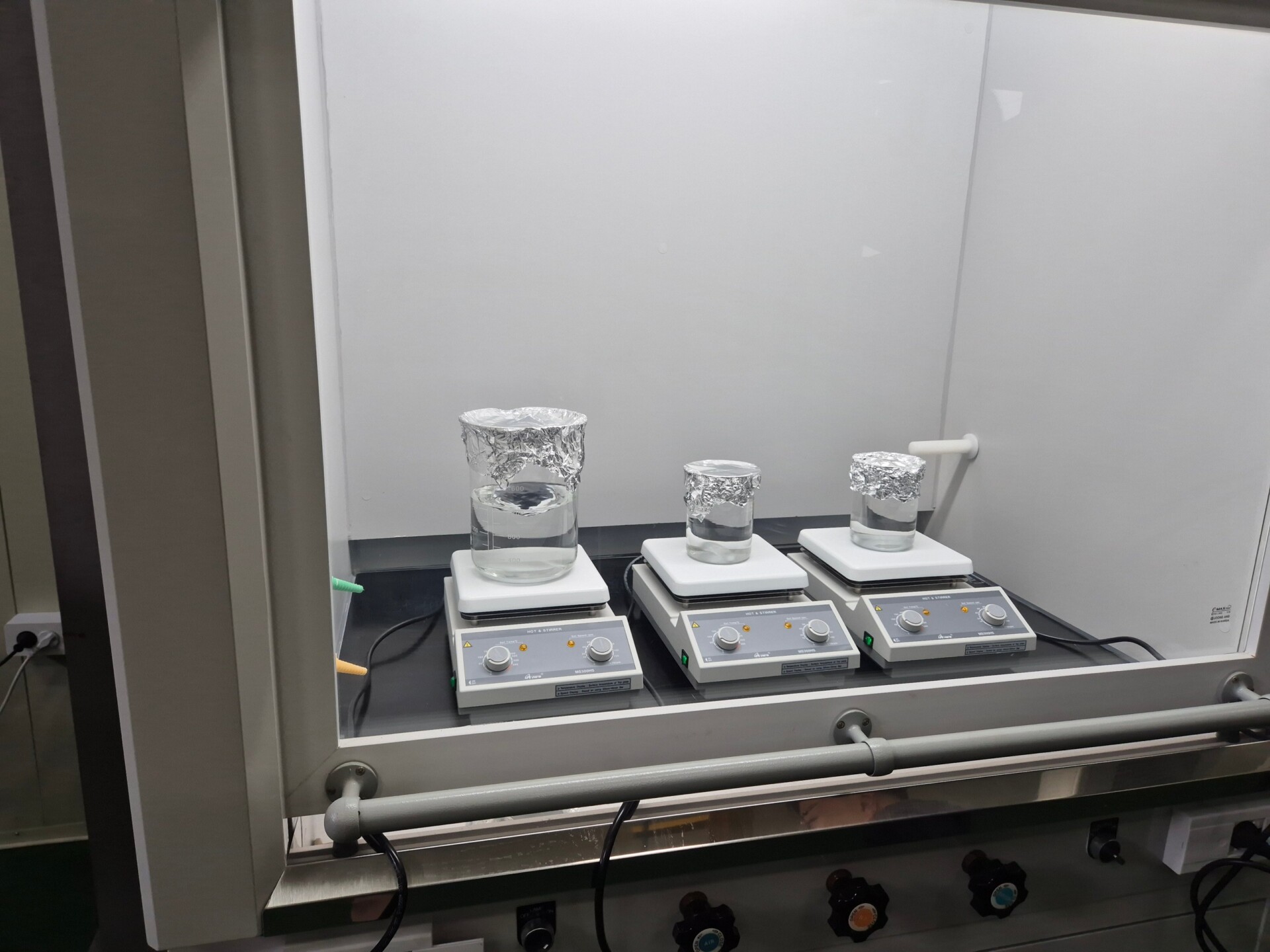
Equipment
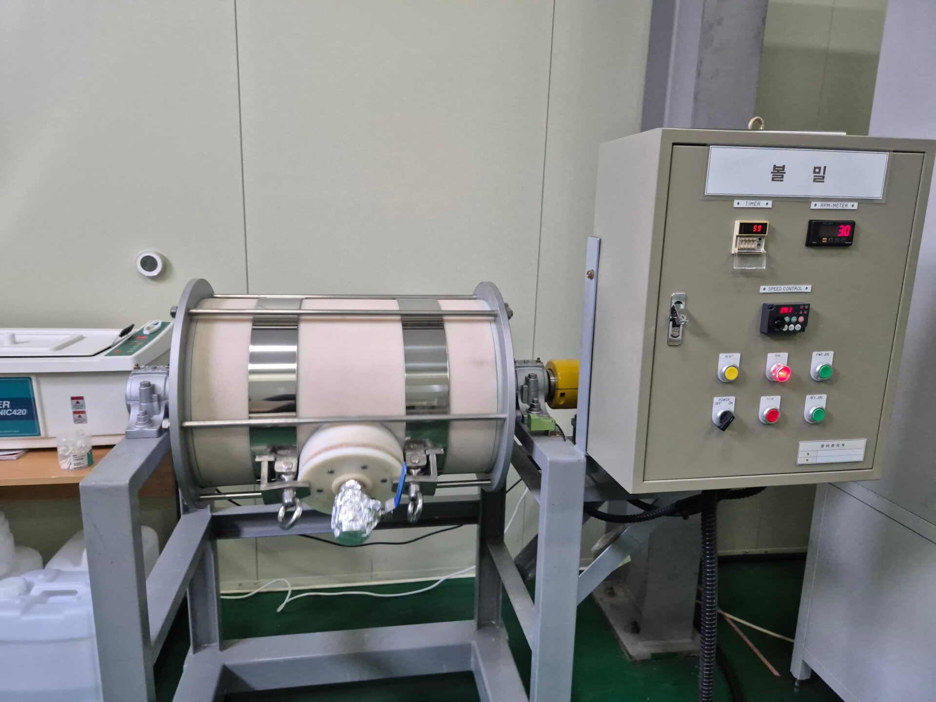
Ball Mill
Material distribution and enhancement of ceramic properties
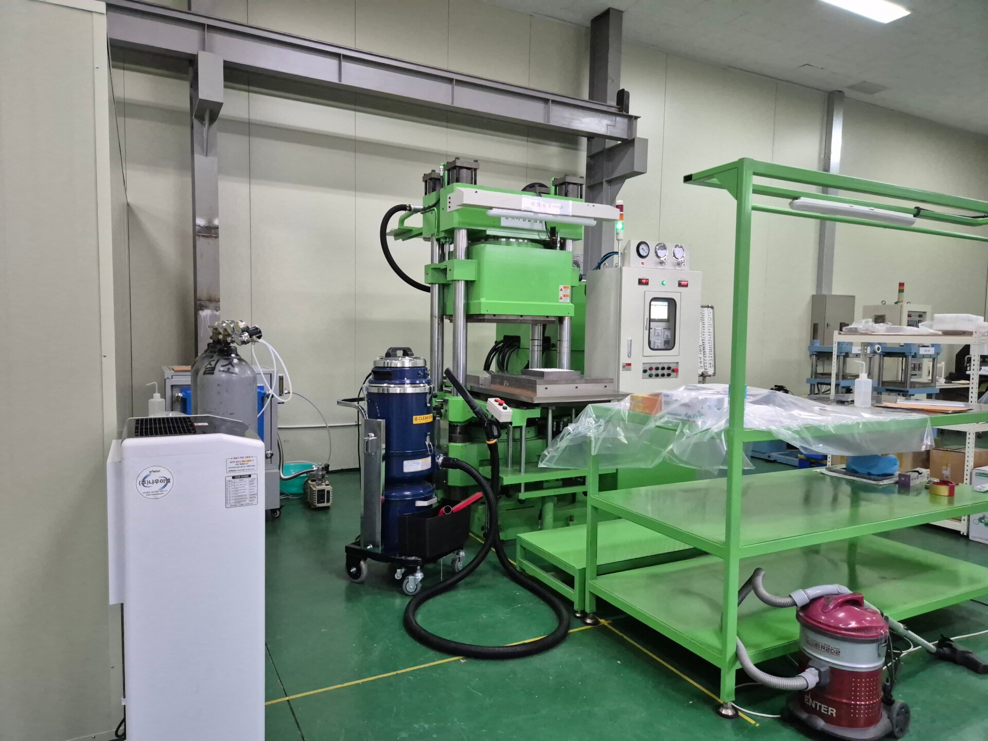
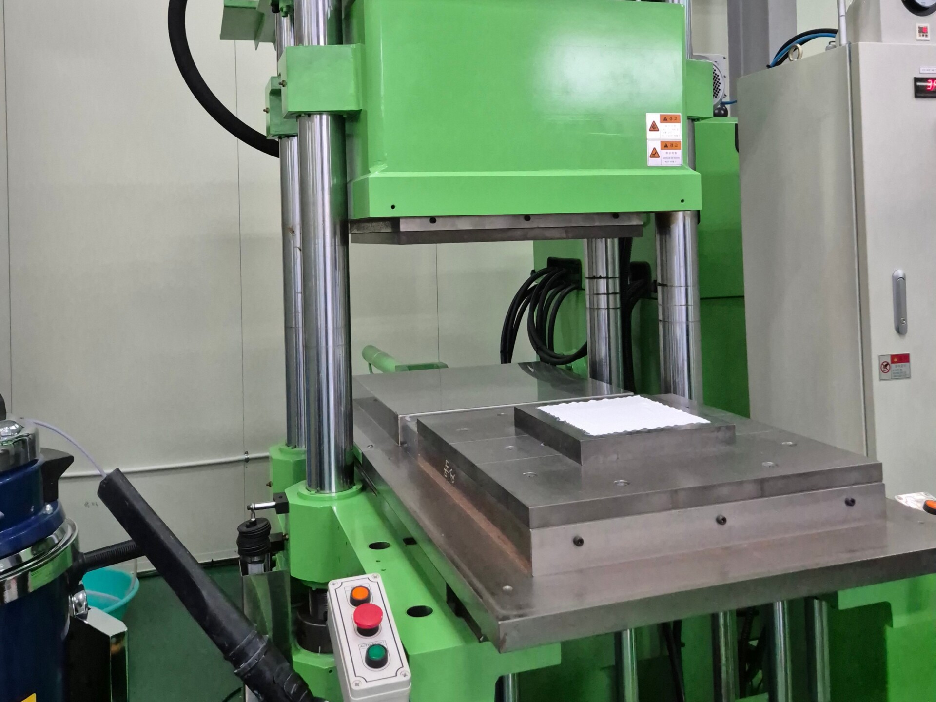
Precision Molding Equipment
Precision shaping of materials
Atmospheric Precision Molding Equipment
Precision shaping of material by control of atmosphere
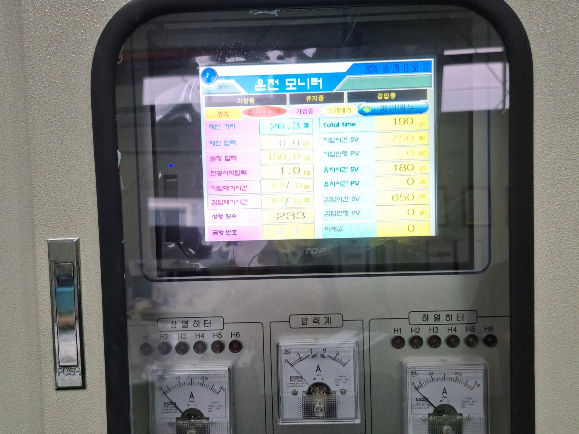
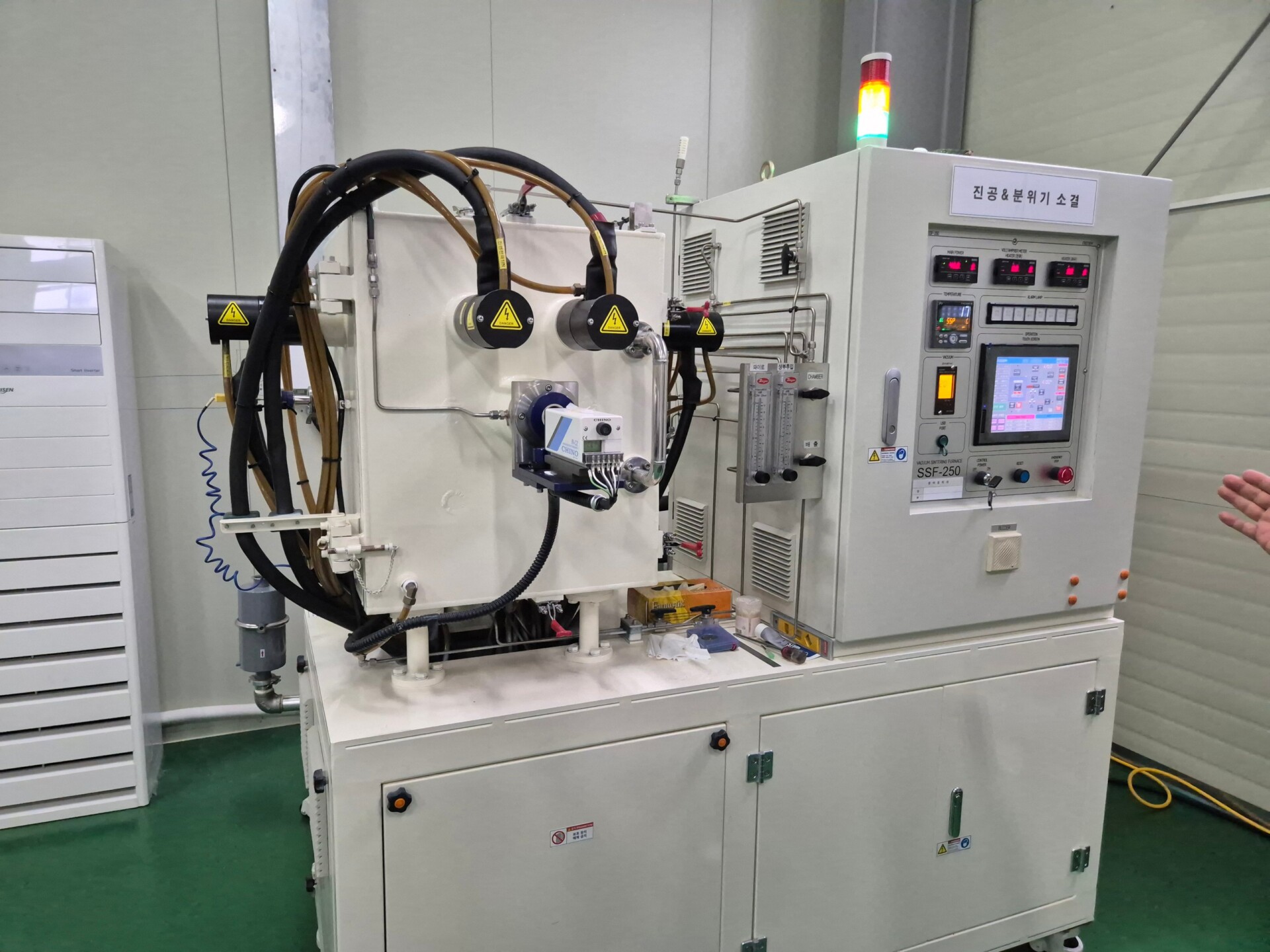
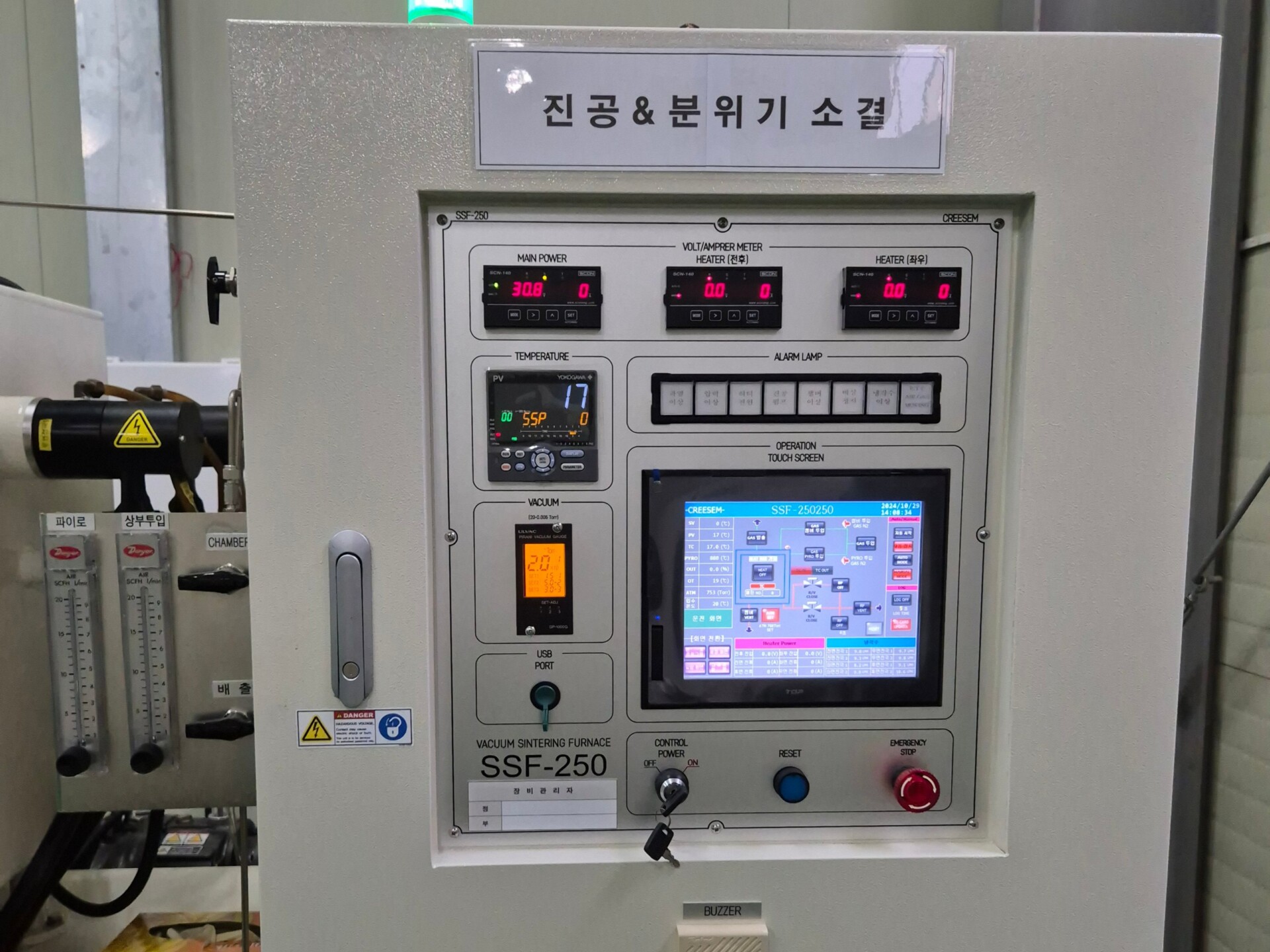
Atmospheric Pressure Sintering Furnace
Sintering of silicon nitride substrate, Control of microstructure
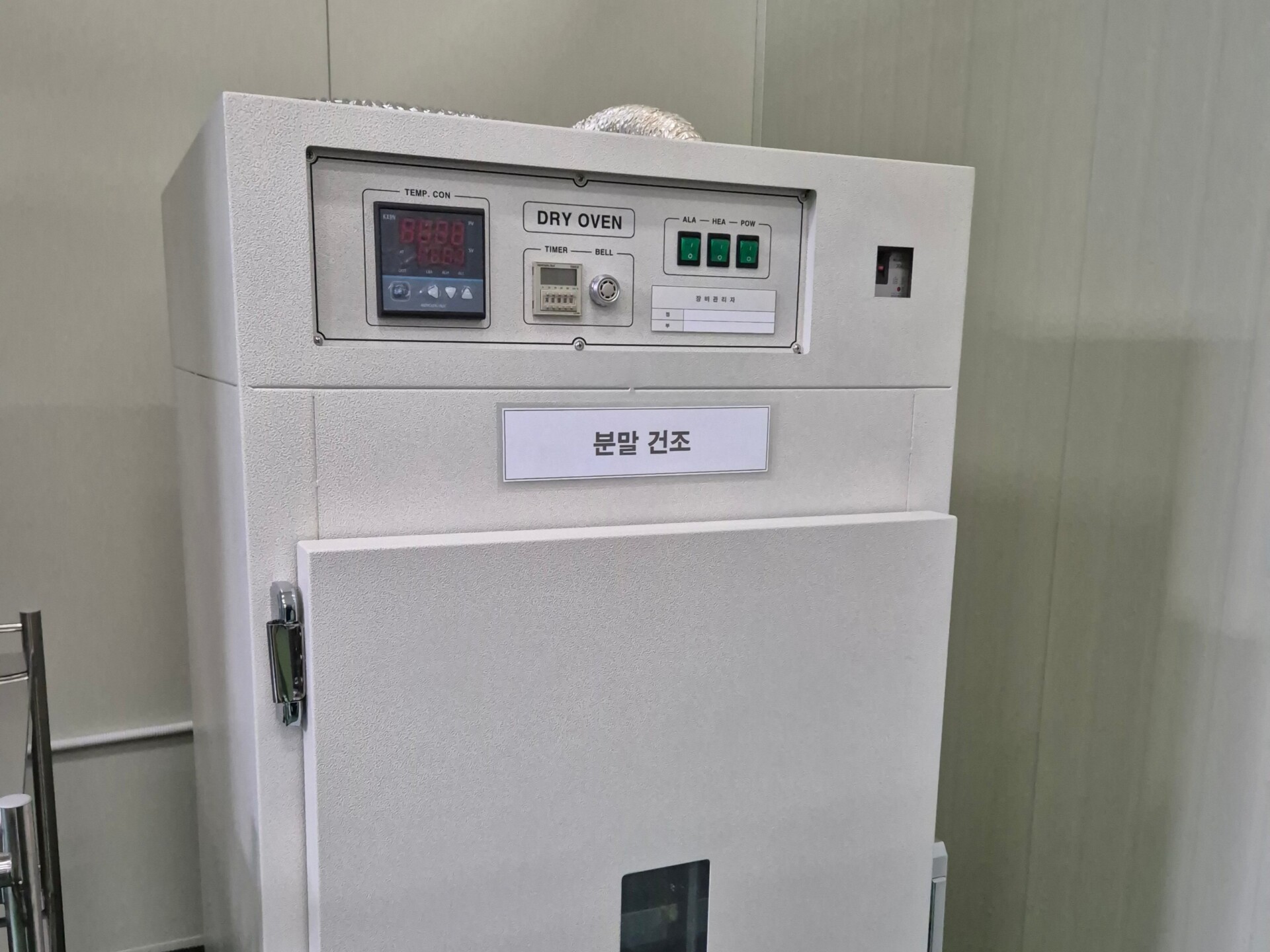
Vacuum Furnace for De-organic
Removal of organic composition under controlled gas conditions
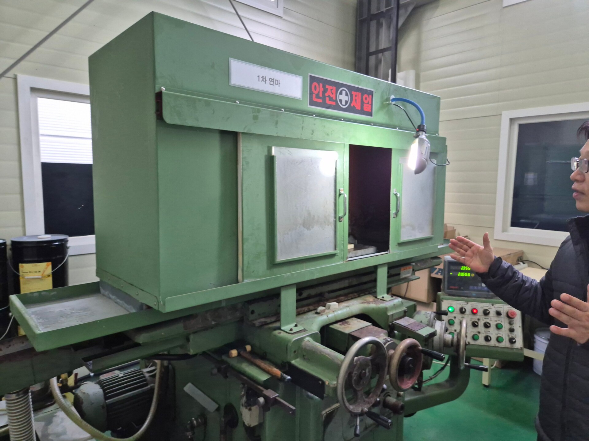
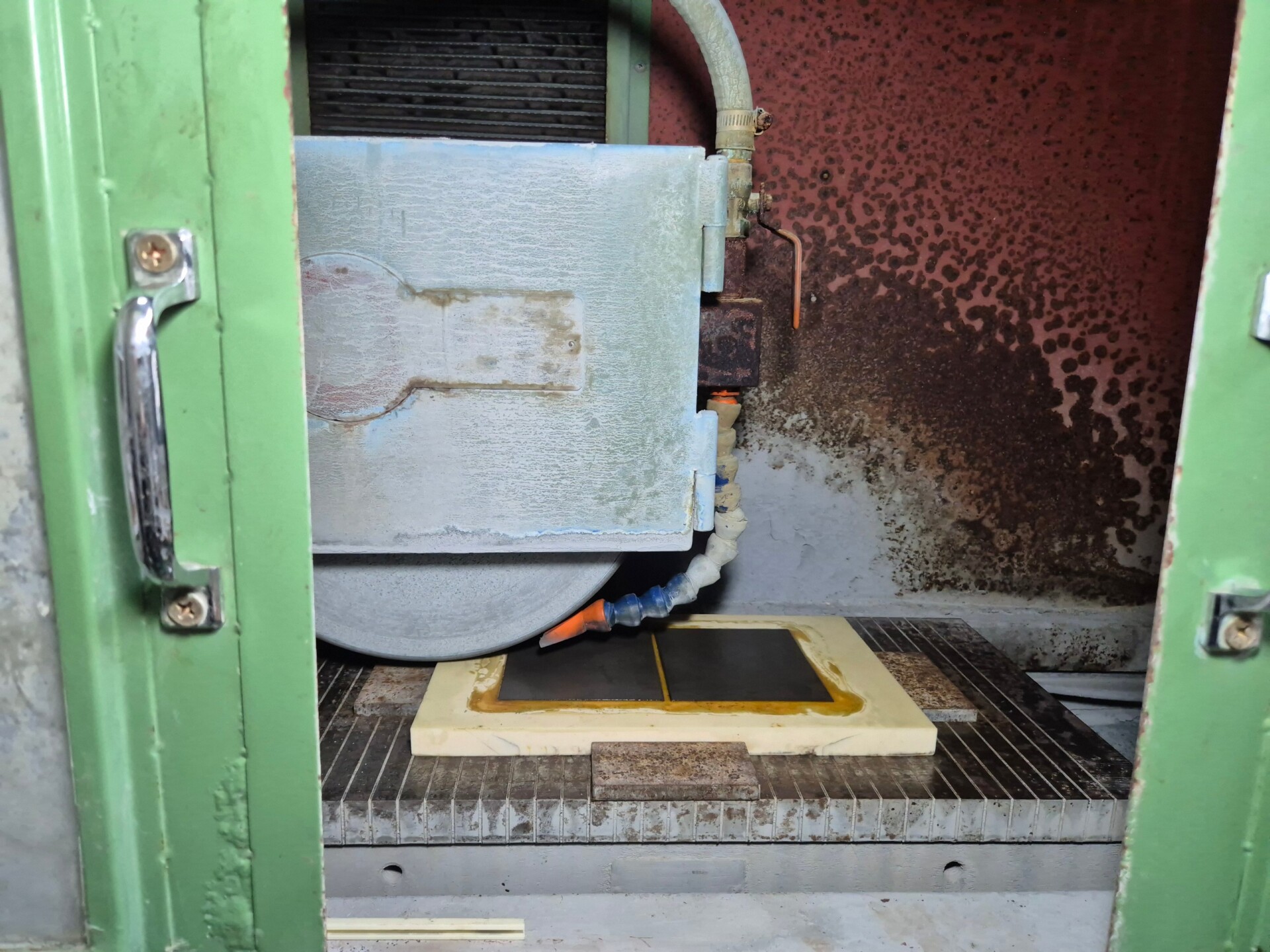
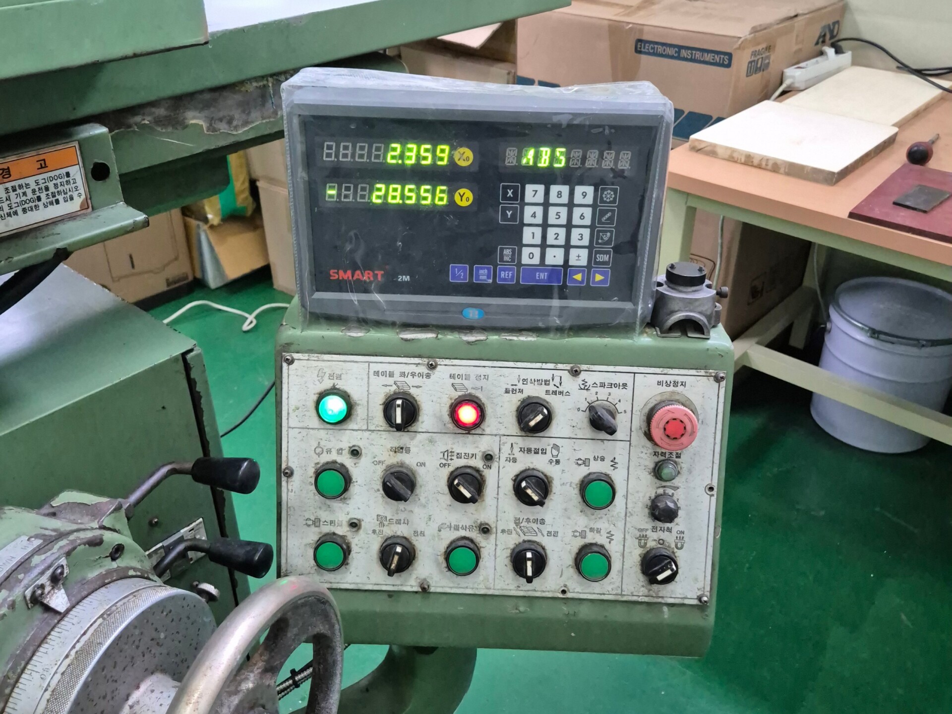
Grinding machine
Surface grinding for inspection of micro-structure
Precision Electronic Scale
Precise weight measurement
Hydrometer
Measuring material density in liquids
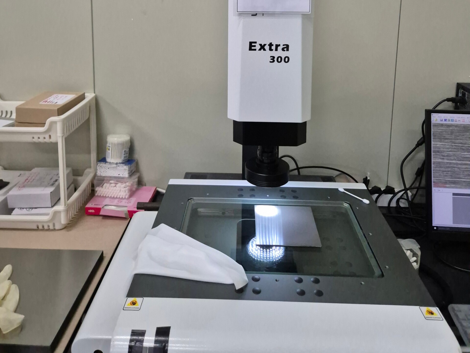
3D Vision Measuring Device
Inspection of micro-structure and defects
Certification
No. 0
Certified Material Specialist Company
No. 0
Venture Business Certification
Company History
2020
November
Established as a specialized corporation for semiconductor equipment materials and components.
2021
January
Initiated development and business for silicon nitride substrates for semiconductor and display inspection equipment.
2021
August
Formed a partnership network for lapping, laser hole processing, and other collaborative needs.
2021
December
Obtained Venture Business Certification (Certification No. 2021155030188)
2022
February
Certified as a Root Enterprise (Certification No. 221212-124143) and as a Specialized Materials Company (Certification No. 27761).
2022
September
Completed product market testing.
2023
December
Conducted an R&D project for sustainable next-generation product development with government funding (approx. $149,000 USD).
2024
January
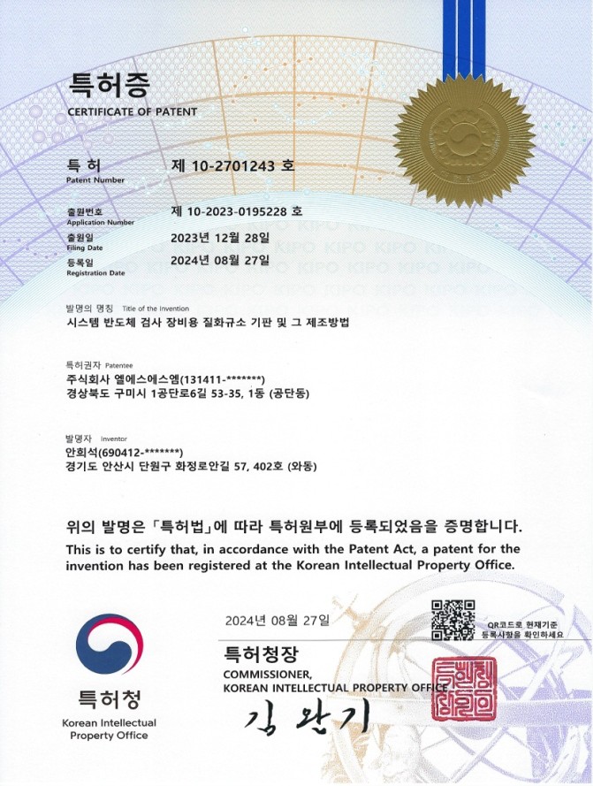
Secured patents and participated in the SEMICON Korea Exhibition.
2024
June
Established an international business partnership network.
2024
October
Ongoing R&D project funded by the Ministry of SMEs and Startups (approx. $74,000 USD).
Contact Us
Your Professional Silicon Nitride Probe Guide Partner. Precision begins with us.